Vitro Shard
Vitro Shard
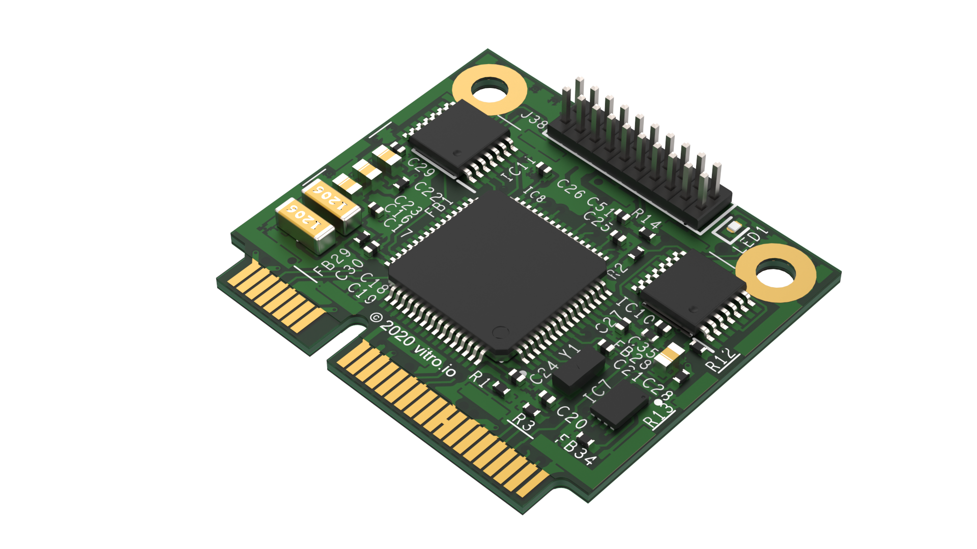
Vitro Shard (v{shard_rev}) is a Computer on Module that delivers an edge to cloud hardware and software solution to secure data from sensors, scanners, scales, and meters in-transit and at-rest in the cloud. Vitro IoT Block libraries enable rapid development of applications serving authenticated data payloads via Zero Trust policies. Its codebase is written in MbedOS/C++ and includes libraries for OTA, AWS IoT integration, ECC authentication, and sample projects. Vitro Shard is built in half mini PCIe form factor for easy integration into other projects.
It is compatible with Vitro Crystal gateway from the local CAN bus to Vitro Cloud infrastructure, and supports over-the-air update services. It comes in mini PCIe card format.
Overview
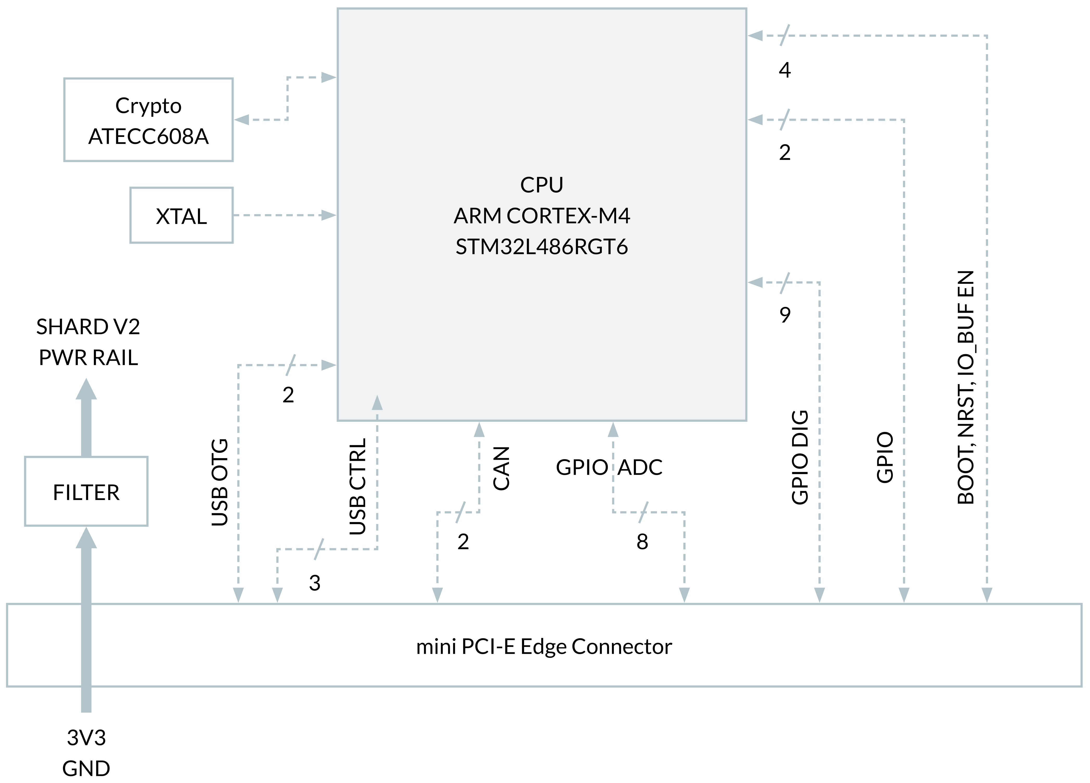
The Vitro Shard has mainly two elements: STM32L486RG MCU and ATECC608A. The device also has up to 8x Analog Input channels 12-bit ADC 5 Msps, up to 16-bit with hardware oversampling, 200 μA/Msps. Regarding digital inputs, it supports CAN (2.0B Active), SPI, USB (OTG 2.0 full-speed, LPM and BCD), 2x I2C, and 3x UART.
Info: Please refer to the Pinout mapping table for more details.
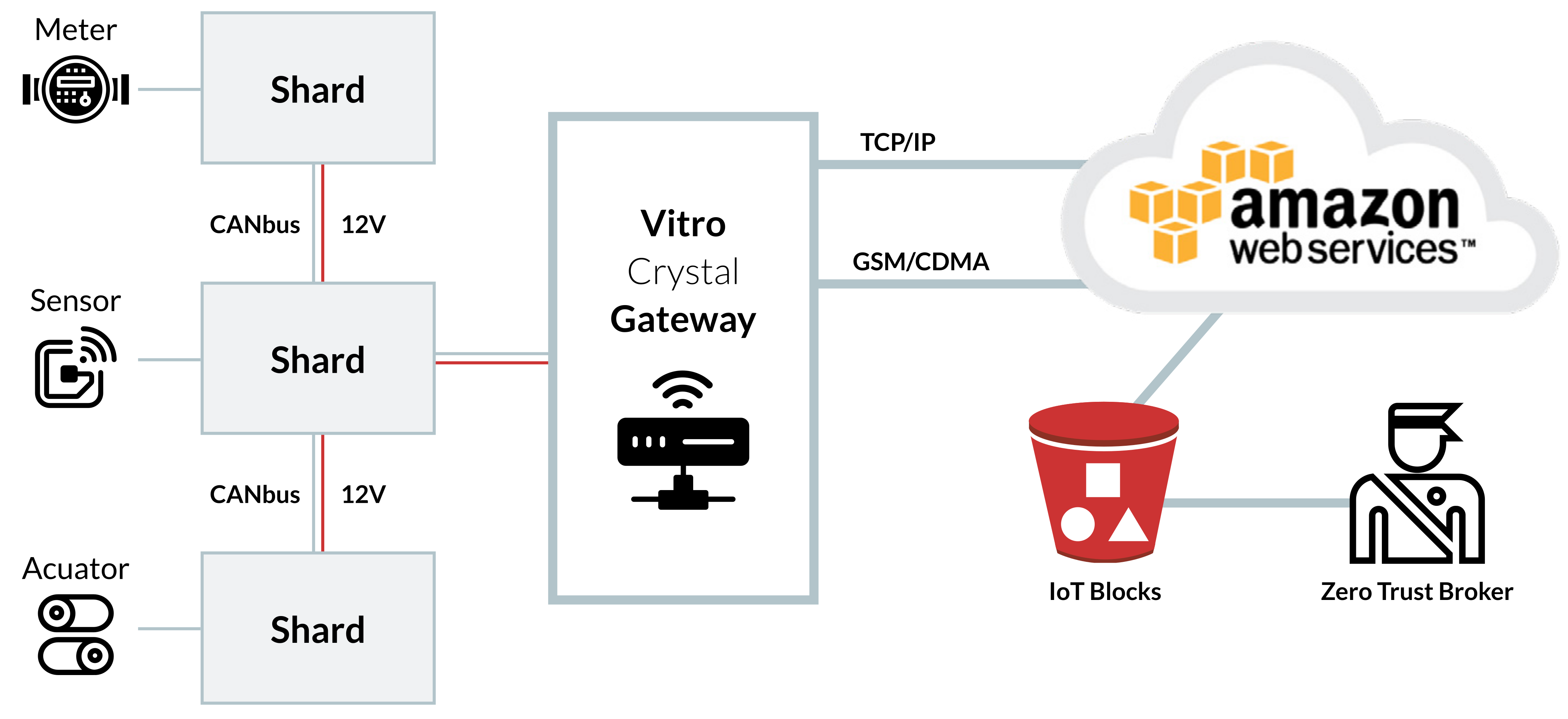
As an example of a typical application for Vitro Shard, you can check the following image:
MCU
The STM32L486RG is an ultra-low-power microcontroller based on the high-performance Arm Cortex-M4 32-bit RISC core. It operates at a frequency of up to 80 MHz, and has 128KB SRAM, 1 MB flash, two banks read-while-write for remote OTA, true random number generator, and AES 256-bit key encryption hardware accelerator.
The Cortex-M4 core features a Floating point unit (FPU) single precision, which supports all Arm single-precision data-processing instructions and data types and implements a full set of DSP instructions and a memory protection
unit (MPU), which enhances application security.
Depending on the selected power-saving mode, different power consumption levels on the CPU unit can be achieved, as low as 420 nA Standby mode with RTC.
The AES hardware accelerator can be used to encipher and decipher data, supports 128-bit block cipher, and the following block cipher mode: ECB, CBC, CTR, GCM, GMAC, and CMAC.
Info: You can learn more by reading the MCU's datasheet and the reference manual.
A simplified block diagram is shown below:
System Memory Boot Mode
The bootloader primary purpose is to download the application program to the internal Flash memory through a serial communication channel. It is stored in the internal boot ROM of any STM32 device.
This means that if you want to flash the MCU via USB or other serial peripheral, it is necessary to enter into bootloader mode. Each serial interface and MCU has its communication protocol. You can obtain this configuration by checking system memory boot mode documentation. Note that the MCU used on Vitro Shard is STM32L486RG, this means that it is in the STM32L47xxx/48xxx family. Information regarding the bootloader of these devices is located in chapter 62, page 328. There, you can verify that the bootloader is activated by applying Pattern 7, which is described in Table 2. The following table is an excerpt from Table 2:
| Pattern | Condition |
|---|---|
| Pattern 7 | Boot0(pin) = 1, nBoot1(bit) = 1 and BFB2(bit) = 0 |
| Pattern 7 | Boot0(pin) = 0, BFB2(bit) = 1 and both banks do not contain valid code |
| Pattern 7 | Boot0(pin) = 1, nBoot1(bit) = 1 and BFB2(bit) = 1 |
Info: Different boot modes can be selected through
BOOT0pin, boot configuration is set bynBoot1bits, andBFB2bit selects boot from Flash memory bank 2.
On Vitro Shard, you can set these pins in the following way:
BOOT0pin should be physically connected with the3.3Vpin output. Vitro Shard Edge has these two pins available on the J64 header.- The Option Byte'nBoot1' bits are set to 1 by default, so no configuration is needed.
- The Option Byte'BFB2' bits can be either 0 or 1; thus, no further actions are needed.
Another important aspect is to connect the serial peripheral correctly with the MCU. For the USB connection, we need to connect it as shown in Table 133 on the DFU bootloader section (found on the system memory boot mode documentation). You can check the USB DFU protocol for this bootloader here.
Secure Boot
You can implement secure boot using Vitro Shard. There are many implementation steps; however, you also need to configure the MCU to make the bootloader immutable, thus becoming the Root of Trust. The necessary configuration is as follows:
- Option bytes must be set to enable Readout protection to level 2.
Warning: This can be done by following the instructions in section 3.5.1 in the reference manual.
- Option bytes must be set to configure the bootloader's memory area as Write Protected.
Warning: The MCU allows you to set a start and end offset to the write-protected area (up to two). The Option Bytes are
WRPxA_STRTandWRPxA_END, wherexcan be either 1 or 2. For more information, check section 3.5.3 in the reference manual.
- Option bytes must be set to enable booting from flash memory only.
Warning: For instructions, please check section 2.6.1 in the reference manual.
These changes will make Vitro Shard always boots from flash memory and hence bootloader. The bootloader can't be changed or erased, but the remaining flash memory can still be reprogrammed.
ST-LINK
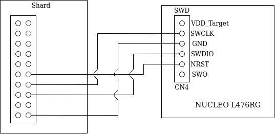
The MCU also supports ST-LINK, which is an in-circuit debugger and programmer. There is no SWD header for Vitro Shard; however, it is available on the device. To do that, you need to add a 2x10 1.27mm male pin header on J38 (FTSH style). Now you can make an SWD connection. As an example, the wiring diagram between Vitro hard and Nucleo L476RG is as follows:
Info: For more information regarding the FTSH style header, you can read the datasheet.
It is recommended that you read ST-LINK utility software documentation, and the user manual.
ECC
The Microchip ATECC608A is a cryptographic co-processor. It integrates ECDH security protocol and ECDSA sign-verify authentication. ATECC608A also has an integrated AES hardware acceleration and enables secure boot capabilities for some MCUs. It also supports autonomous PKI key generation and storage for up to 16 keys, certificates, and data.
There is also hardware support for asymmetric sign, verify, and key agreement; and for symmetric algorithms (e.g., SHA-256 and AES-128). The chip offers full ECDSA code signature validation and optional stored digest/signature for secure boot. There are security features to better protect from attacks: optional communication key disablement prior to secure boot, and encryption/authentication for messages to prevent onboard attacks.
There are many differences between Vitro Crystal's ATECC508A and Vitro Shard's ATECC608A. They are listed in sections 3.1.1 and 3.1.2 of the ATECC608A Data Sheet.
Ratings
The ratings of the device are as follows:
| Parameter | Symbol | Min | Max | Unit |
|---|---|---|---|---|
| Supply Voltage | V_DD | -0.3 | 4.0 | V |
| FT GPIO Input Voltage | FT GPIO V_IN | -0.3 | V_DD + 4.0 | V |
| TT GPIO Input Voltage | TT GPIO V_IN | -0.3 | 4.0 | V |
| BOOT0 Pin | V_N BOOT0 | -0.3 | 9 | V |
| Operating Ambient Temperature | T_AMB | -40 | 85 | °C |
Warning: Stresses above the absolute maximum ratings listed above may cause permanent damage to the device. These are stress ratings only and functional operation of the device at these conditions is not implied. Exposure to maximum rating conditions for extended periods may affect device reliability.
Electrical Characteristics
Specifications apply for –40°C < T_PCB < 85°C, unless otherwise noted.
| Parameter | Symbol | Min | Typical | Max | Unit |
|---|---|---|---|---|---|
| Supply Voltage | V_DD | 2.0 | 3.3 | 3.6 | V |
| FT GPIO Input Voltage | FT_V_IN | 5.5 | V | ||
| TT GPIO Input Voltage | TT_V_IN | 3.6 | V | ||
| Voltage Input High | V_IH | 0.7V_DD | V | ||
| Voltage Input Low | V_IL | 0.39V_DD | V | ||
| Voltage Output High | V_OH | V_DD - 0.44 | V | ||
| Voltage Output Low | V_OL | 0.4 | V |
Pinout
The pinout tables are:
Power
| Pin # | Net Name | Pin Style | STM32 Pin # | STM32 Pin Name | Alternate Function | IO Voltage Group |
|---|---|---|---|---|---|---|
| 2, 24, 39, 41, 52 | 3V3 | PWR | ||||
| 4, 9, 18, 26, 34, 35, 37, 40, 50 | GND | GND |
NC
| Pin # | Net Name | Pin Style | STM32 Pin # | STM32 Pin Name | Alternate Function | IO Voltage Group |
|---|---|---|---|---|---|---|
| 11, 13, 16, 23, 25, 31, 33 | NOT CONNECTED | NC |
RSVD
| Pin # | Net Name | Pin Style | STM32 Pin # | STM32 Pin Name | Alternate Function | IO Voltage Group |
|---|---|---|---|---|---|---|
| 22 | NRST | RSVD | ||||
| 20 | BOOT0 | RSVD | ||||
| 43 | IO_BUF_EN | RSVD | 2 | PC13 | OUTPUT/RSVD | FT / 5V Tolerant |
| 44 | IO_BUF_EN HARD3V3 | |||||
| EN_N_PC3 | RSVD | 11 | PC3 | GPIO | FT / 5V Tolerant |
IO
| Pin # | Net Name | Pin Style | STM32 Pin # | STM32 Pin Name | Alternate Function | IO Voltage Group |
|---|---|---|---|---|---|---|
| 36 | USB_OTG_FS_DM | USB | 45 | PA12 | GPIO/USB_DM | FT / 5V Tolerant |
| 38 | USB_OTG_FS_DP | USB | 44 | PA11 | GPIO/USB_DP | FT / 5V Tolerant |
| 42 | USB_OTG_FS_VBUS_PA9 | USB | 42 | PA9 | GPIO/USB_VBUS | FT / 5V Tolerant |
| 21 | USB_OTG_OVRCR_BUF | USB | 34 | PB13 | INPUT | FT / 5V Tolerant |
| 29 | USB_OTG_PPWR_BUF | USB | 37 | PC6 | OUTPUT/USB_PWR_EN | FT / 5V Tolerant |
| 27 | USB_OTG_PRDY_BUF | USB | 34 | PB13 | INPUT | FT / 5V Tolerant |
| 10 | CAN_RX_BUF | GPIO | 61 | PB8 | INPUT/CAN_RX | FT / 5V Tolerant |
| 8 | CAN_TX_BUF | GPIO | 62 | PB9 | OUTPUT/CAN_TX | FT / 5V Tolerant |
| 28 | SPI1_MISO/ADC1_IN11 | GPIO | 22 | PA6 | GPIO/SPI/ADC | FT / 5V Tolerant |
| 6 | SPI1_MISO/ADC1_IN12 | GPIO | 23 | PA7 | GPIO/SPI/ADC | FT / 5V Tolerant |
| 46 | SPI1_NSS/ADC1_IN9 | GPIO | 20 | PA4 | GPIO/SPI/ADC | FT / 3.6V Tolerant |
| 48 | SPI1_SCK/ADC1_IN10 | GPIO | 21 | PA5 | GPIO/SPI/ADC | FT / 3.6V Tolerant |
| 7 | UART_DEBUG_RX | GPIO | 54 | PD2 | GPIO/UART | FT / 5V Tolerant |
| 5 | UART_DEBUG_TX | GPIO | 53 | PC12 | GPIO/UART | FT / 5V Tolerant |
| 12 | UART_RS232_RX_BUF | GPIO | 17 | PA3 | INPUT/UART | FT / 5V Tolerant |
| 14 | UART_RS232_TX_BUF | GPIO | 16 | PA2 | OUTPUT/UART | FT / 5V Tolerant |
| 19 | UART_RS485_DE | GPIO | 27 | PB1 | GPIO/UART | FT / 5V Tolerant |
| 15 | UART_RS485_RX | GPIO | 30 | PB11 | GPIO/UART | FT / 5V Tolerant |
| 17 | UART_RS485_TX | GPIO | 29 | PB10 | GPIO/UART | FT / 5V Tolerant |
| 3 | UART_USER_RX/ADC1_IN6 | GPIO | 15 | PA1 | GPIO/UART/ADC | FT / 5V Tolerant |
| 1 | UART_USER_TX/ADC1_IN5 | GPIO | 14 | PA0 | GPIO/UART/ADC | FT / 5V Tolerant |
| 51 | GPIO_PC10 | GPIO | 51 | PC10 | GPIO | FT / 5V Tolerant |
| 49 | GPIO_PC11 | GPIO | 52 | PC11 | GPIO | FT / 5V Tolerant |
| 30 | I2C1_SCL | GPIO | 58 | PB6 | GPIO/I2C | FT / 5V Tolerant |
| 32 | I2C1_SDA | GPIO | 59 | PB7 | GPIO/I2C | FT / 5V Tolerant |
| 47 | I2C3_SCL/ADC1_IN1 | GPIO | 8 | PC0 | GPIO/I2C/ADC | FT / 5V Tolerant |
| 45 | I2C3_SDA/ADC1_IN2 | GPIO | 9 | PC1 | GPIO/I2C/ADC | FT / 5V Tolerant |
Pinout Details
| GPIO Pin Type | Available Pins within this Group | Description |
|---|---|---|
| GPIO | 2 | General Purpose Input/Output pin – can work either as an output or input |
| GPIO DIG | 9 | Pins from this group can work as a regular GPIO or can work as specific interface lines (SPI/I2C/UART) – refer to pinout mapping table for Digital interfaces location details |
| GPIO ADC | 8 | Pins from this group can work as a regular GPIO or can work as Analog Input pin to ADC |
| CAN | 3 | Pins from this group can work as a regular GPIO or can work as CAN TX/RX interface lines – refer to pinout mapping table for Digital interfaces location details |
| USB | 2 | Pins from this group can work as a regular GPIO or can work as a USB DP/DN differential pair – refer to pinout mapping table for location details |
| USB CTRL | 3 | Pins from this group can work as a regular GPIO or can work as USB CTRL lines together with USB differential pair – refer to pinout mapping table for location details |
| RSVD | 4 | Internal IO buffer enable, STM32 NRST, STM BOOT lines |
Specifications
| Name | Description |
|---|---|
| Microcontroller | ARM Cortex-M4 STM32L4 @ 80 MHz |
| MCU Memory | 1 MB (1M x 8) FLASH |
| Security IC | ATECC608A-MAHDA-T |
| USB OTG | 1 |
| UART Interface | 1x dedicated for RS-485 connection on carrier card |
| UART Interface | 1x dedicated for RS-232 connection on carrier card |
| UART Interface | 1x dedicated for Debug interface on carrier card |
| UART Interface | 1x dedicated for user usage (switchable UART/ADCIN) |
| SPI Interface | 1x dedicated for user usage (switchable UART/ADCIN) |
| I2C Interface | 1x dedicated for user usage (switchable I2C/ADCIN) |
| I2C Interface | 1x dedicated for internal usage |
| Status LEDs | 1 |
| I/O | 10X GPIO PINS (multifunction pins: GPIO/I2C/SPI/UART/ADC) |
| Power Input | 3.3V DC via miniPCIE slot |
| Temperature Range | Commercial: 0°C to 85°C |
| Temperature Range | Industrial: -40°C to 100°C (optional) |
| Mechanical/Board Size | Standard Half-size mini-PCIe board size |
Updated about 1 year ago